Chemical-mechanical planarization (CMP) is a crucial step in semiconductor manufacturing, required for producing advanced AI chips. My assessment is that China’s tools, primarily those from the leading Chinese firm Hwatsing, are good enough to produce indigenous HBM3, China’s near-term target. I would bet that this indigenization progress will continue, and that wafer polishing will not be a bottleneck for China’s AI chip ambitions. [...]
In this post, I first explore the basics of CMP, how it works, and its role in HBM production. I then examine what makes CMP for advanced packaging difficult and how China’s capabilities stack up against their Western equivalents. I next dive into China’s CMP supply chain, exploring Hwatsing in depth, along with its two key competitors. I conclude with a summary of the outlook for China’s CMP industry and open questions about hybrid bonding.
Flat wafers are good wafers
CMP plays a simple but important role in semiconductor production, accounting for 6% of the hundreds of steps involved in wafer processing. After patterning with photolithography, etching away material, and depositing new materials, there is a need to tidy up. The silicon wafer, with these layers of new material on top, needs to be flattened so that a new layer can be formed. As the name suggests, CMP tools do this through a combination of abrasive chemicals and physical polishing. This sounds simple but is difficult in practice because it requires an incredibly high standard of planarization—creating an ultra-smooth, flat surface—while avoiding impurities, scratches, and other defects that can easily emerge when grinding away material.
CMP is needed for all the major elements of HBM production: producing the DRAM dies and base dies that were the subject of the first piece in the series, as well as the through-silicon vias explored in the second piece, and the advanced packaging stages that integrate HBM into the wider chip. Different stages are more or less difficult depending on the material being removed and how much needs to be removed. For example, removing large volumes of copper at high throughput with precision is trickier than removing a more even, thinner layer of dielectric material.
A CMP tool is split into CMP modules and cleaning modules. A diagram is below, but in simple terms, the wafer is placed inside a polishing head, which holds it in place and then rotates it over a specially designed pad covered in abrasive chemical slurries that strip away material. It is a chemical process because the materials in the slurry react with the materials in the wafer, softening or removing them. It is also a mechanical process because the wafer is physically pressed down onto the pad, so that particles on the wafer, softened by the chemicals, can be peeled away. The force is kept as low as possible to avoid damaging the structures on the wafer.
One analogy is rubbing rust off a piece of metal, where exposure to oxygen has produced an oxide variant that is more easily removed. This is how CMP works with materials like copper, just at a much faster and more controlled rate.
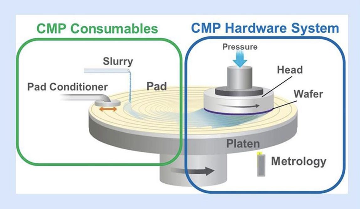
CMP has a reputation as a dirty process that generates large numbers of unwanted particles, hence the need for the cleaning modules. Rather than the pure vacuum chambers and sci-fi techniques of photolithography or etching, the wafer is sloshed around in chemicals and ground down. So the main risk of CMP is that it introduces impurities or defects into the wafer, which can severely reduce the yield of the process line—the share of chips that come out working. Small impurities from CMP can carry over to other process stages and tools, causing wafers to be defective and discarded.
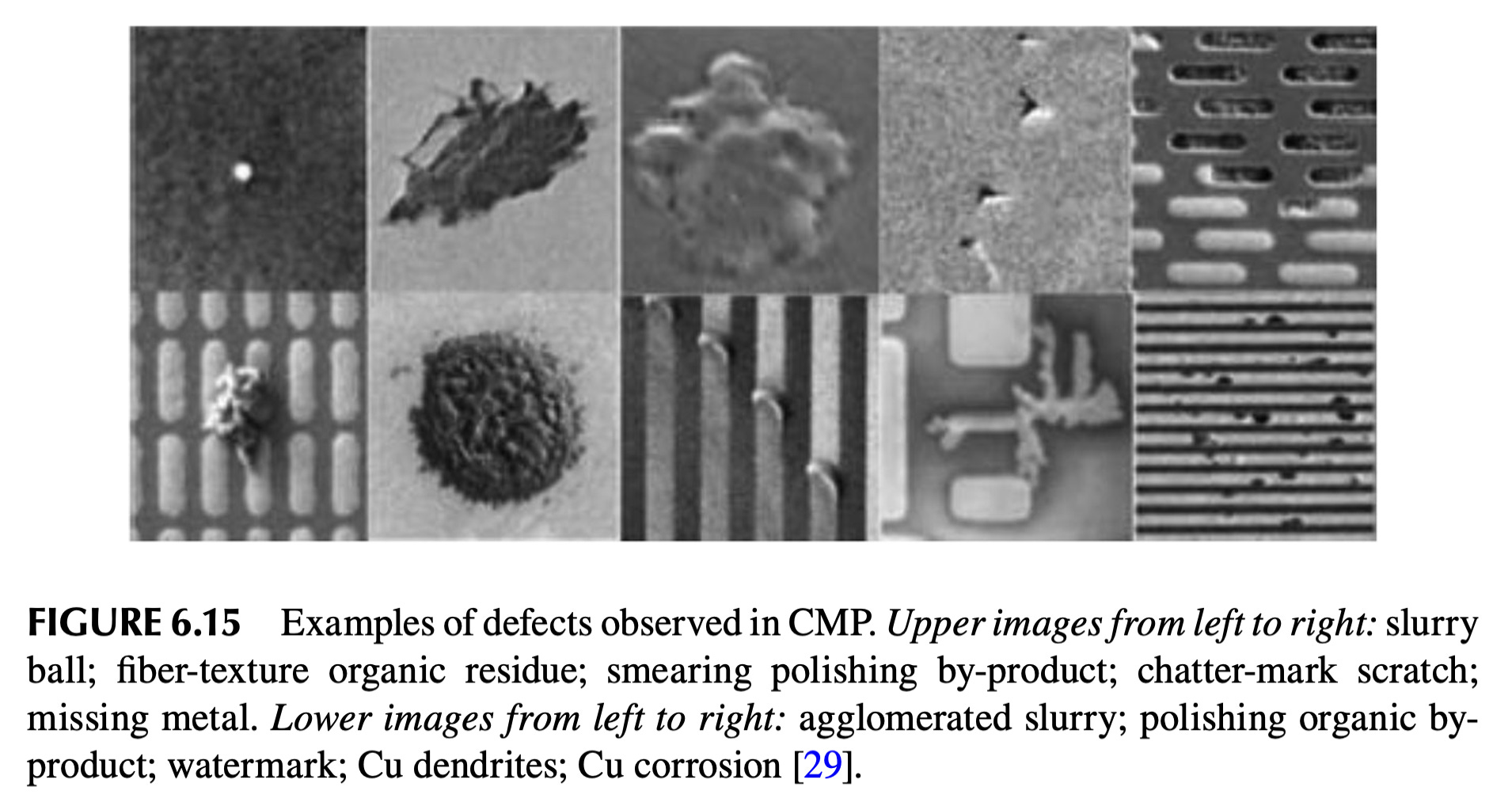
The best CMP tools introduce as few impurities or defects as possible and have robust integrated cleaning modules to remove any that do get introduced before they degrade the production line’s yield. CMP for advanced nodes just raises the necessary level of precision and cleanliness. Ever smoother surfaces are needed, at good throughput, and without even a speck of a particle.
CMP is not just about the tool, however; it also involves consumable inputs. The pad on which the wafer is polished needs to be replaced often, after just 400-800 wafers, depending on the material. A large DRAM fab will process more than 100,000 wafers a month, with CMP required at many stages, meaning thousands of replacement pads a month. The slurry needs to be tuned to the exact process requirements, ensuring the right chemical mix for the materials on the wafer. These consumables need to be highly consistent so that small changes in the chemical composition of the slurry, for example, don’t upset the CMP tool’s parameters. [...]
Demands on CMP are likely to rise further due to the move towards hybrid bonding. Currently, the TSVs in all the DRAM dies are stacked using solder microbumps. These are little blobs of metal that connect the TSVs, and are usually formed using a process called thermo-compression bonding. Microbumps do the job but are undesirable. They increase the stack height, reducing the number of DRAM dies that can fit. They are also worse than hybrid bonding in the density of interconnections they enable and in their power efficiency.

Hybrid bonding leaves little room for error. The copper bond pads for the TSVs need near-perfect alignment, and there can be almost no impurities between them; otherwise, you will disturb the bond. CMP is critical because the two dies need to be as flat and level as possible so they can be properly bonded. While solder bumps can get away with accuracy at the micron level, hybrid bonding needs surface polishing down to 0.5 nanometer precision, orders of magnitude finer. [...]
CMP tools are unlikely to be a bottleneck to China scaling up its indigenous production of HBM3. For the required DRAM and advanced packaging steps, Hwatsing and, in a couple of years, AMEC-Zhonggui will have capable tools. The core bottleneck for domestic HBM3 production will remain in other areas, primarily photolithography. [...]
Hybrid bonding is how this would be accomplished, and the best hope for Chinese memory firms to leapfrog and close the performance gap.
by Hamish Low, The Substrate | Read more:
Images: Planarization for Advanced Packaging and Hybrid Bonding. AMA Packaging Master Class
[ed. Learn something new every day. See also: What would make a large US lead in AI good or bad for the world? (Substrate):]***
"Right now, the US leads over China in AI. Yes there is a lot of nuance to that statement, and yes China does have advantages in areas like energy production and humanoid robotics, but on the whole it’s obvious that the US is in some sense ahead in AI.My current best guess is that this is very good. I think a large US lead over China is better for the world (not just for the US), and that a shrinking US lead would be bad. A large lead gives US companies and the US government more room to test frontier AI systems, make them secure, and avoid panicked decisions. I also think it’s better if frontier AI development happens mostly in a pluralistic, open society with checks and balances.
[What do I mean by “good (or bad) for the world”? I basically have in mind a period where: there’s no new great power conflict or world war; AI is developed safely and responsibly; there’s no extreme power concentration and values aren’t permanently locked in; and AI enables broad prosperity and flourishing, in the way that past technological progress since the Industrial Revolution has made the world better overall.]
What do I mean by “lead”, anyway? I don’t think we need a precise definition to make progress here, but what I have in mind is roughly a gestalt comprising many different factors: AI model capabilities, the capabilities of entire AI systems (including agent harnesses), compute and other infrastructure, capital and customer bases, and more generally the strength of each country’s broader AI ecosystem. In addition to technical capabilities, it matters how technical capability is converted into power, e.g., as measured by AI adoption in industry and government. The actual lead is of course very jagged and any single measure of it is reductive (more on that in a moment), but broadly speaking, the country in the lead will control more, and more capable, AI systems, and will have a military and economic advantage as a result."
What do I mean by “lead”, anyway? I don’t think we need a precise definition to make progress here, but what I have in mind is roughly a gestalt comprising many different factors: AI model capabilities, the capabilities of entire AI systems (including agent harnesses), compute and other infrastructure, capital and customer bases, and more generally the strength of each country’s broader AI ecosystem. In addition to technical capabilities, it matters how technical capability is converted into power, e.g., as measured by AI adoption in industry and government. The actual lead is of course very jagged and any single measure of it is reductive (more on that in a moment), but broadly speaking, the country in the lead will control more, and more capable, AI systems, and will have a military and economic advantage as a result."

